


Plasma Nano Coating
This physical vapor deposition (PVD) process uses plasma ions with high energy in a high-vacuum atmosphere to form a deposition layer of multiple ㎚ to ㎛ on a product surface. It can be used to coat a variety of materials including metals, alloys, and ceramics.
| Item | Plasma Nano Ncoating | Note |
|---|---|---|
| Roughness(Ra) | 4? or higher | Affected by the roughness of base metal |
| Porosity (%) | Less than 0.2% | |
| Hardness(Hv) | - | No surface scratches at 9H of pencil hardness |
| Adhesion(MPa) | 19.9 Mpa or higher | Bonding material separation value (thermal spray layer of16.1Mpa) |
| Volume resistance | 3um(260V,11mA) | 6um(330V,11mA) |
| Color | Translucent yellow | ~10㎛ : transparent 15㎛~ : pale yellow |
| Plasma resistance | Good | 1.4 times as high as Y2O3 thermal spray layer |
| Coating thickness | Multiple nm ~ 20㎛ | Can control thickness in units of Nm |
| Thermal shock | ~ 850℃ | Test completed up to 850℃ |
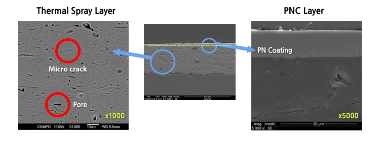
| Category | Thermal Spray Coating | PN Coating | Note |
|---|---|---|---|
| Porosity (%) | 4% | Less than 0.2% | ※ The lower the porosity gets, the more resistant the plasma gets |
| Micro Crack | Yes | No | ※ The lower the micro crack, the less particles |
| Roughness (Ra) | ㎛ unit | Nano unit | |
| Density (kg/㎠) | 165 | 203 or higher (Re-separation of bonding) | ※ Measurement standard of JIS H 8666 |
| Shield capacity | Good | Completely shielded |
Head Office in Gumi Address : (39422) 39 4gongdan-ro 7-gil, Gumi-si, Gyeongsangbuk-do
Tel : 054-473-8968~70 Fax : 054-471-4781 Email : kstgumi@kst1.co.kr COPYRIGHT (C) 2013 KOREA STAR TECH CO,.LTD. ALL RIGHTS RESERVED.
Tel : 054-473-8968~70 Fax : 054-471-4781 Email : kstgumi@kst1.co.kr COPYRIGHT (C) 2013 KOREA STAR TECH CO,.LTD. ALL RIGHTS RESERVED.